Last Updated on 8th March 2023 by peppe8o
In this article, we will explore the main types of PCB pads and their applications, providing valuable insights into the world of electronic circuit design.
Printed Circuit Board (PCB) pads are essential components of any electronic circuit design. These small, conductive areas on a PCB allow for the connection of electronic components to the board, enabling the flow of electrical signals and power.
PCB pads come in a variety of shapes and sizes, each designed for a specific purpose in the circuit design. Understanding the different types of PCB pads and their uses is crucial for designing effective and efficient electronic circuits.
What is a PCB Pad?
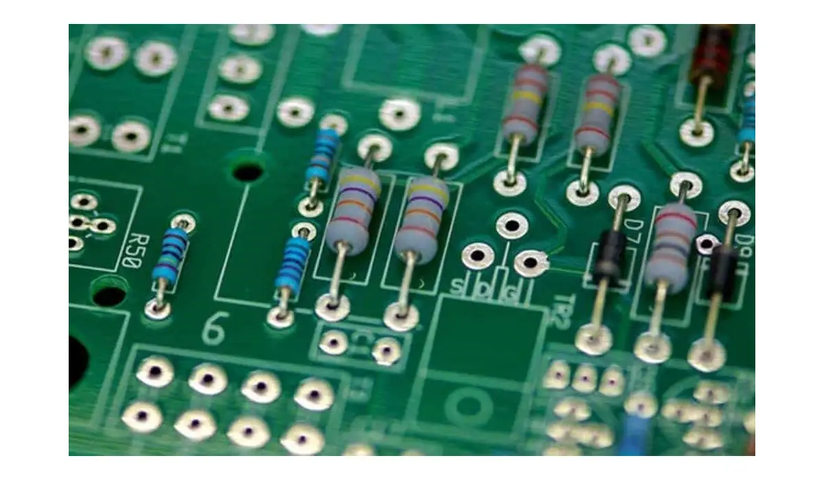
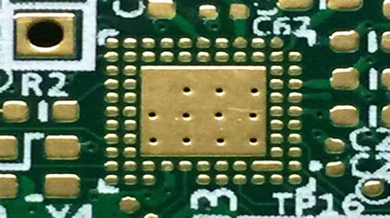
A pad is the exposed area of copper on a circuit board, where the component lead is soldered. The electrical connection of all components is made via pads.
The design and placement of pads directly affect the solderability, stability, and heat transfer of components.
According to different components and packaging methods, PCB pads can be typically divided into through-hole pads and surface mount pads.
Through-hole Pad
The first of our types of PCB Pads is the through-hole pads, used to mount through-hole components. When soldering, the component pins need to be inserted into the via holes of the pad.
Soldering components via through-hole pads can create reliable solder joints between the components and the PCBs, providing a long-term mechanical and electrical connection. However, due to the component leads and the number of holes, the available routing areas on a multilayer board will be limited.
Surface Mount Pad
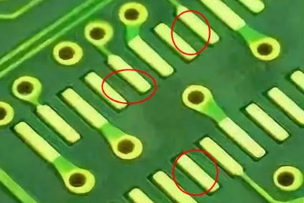
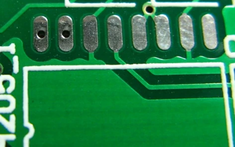
Pads that allow electronic components to be mounted directly on the board surface are called surface mount pads. Unlike through-hole pads, surface mount pads are suitable for mounting smaller components. They allow more components to be placed in a smaller space while providing larger functionality and performance. This type of pad is a great advantage in the design of complex multi-layer boards. However, surface mount pads commonly cannot be used for components that will generate high heat levels.
BGA Pad
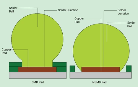
When connecting BGA-style components, the proper pad design is also crucial to ensure the manufacturability of the boards. There are two common types of BGA pads: Solder Mask Defined Pads (SMD) and Non-Solder Mask Defined Pads (NSMD).
Solder Mask Defined Pads (SMD)
SMD pads are defined by the solder mask apertures applied to the BGA pads. In this pad design, the mask aperture is smaller than the actual copper pad, and the pad is partially covered by the surrounding solder mask. The use of SMD pads has some advantages. For example, the overlapping mask helps prevent the pad from shifting or coming off the board. Also, the pad is useful for BGA positioning. However, this type of pad reduces the contact area between the pad and the copper surface, as well as the space between adjacent pads. This limits the thickness of the tracks between the pads and can affect the use of through-holes.
Non-Solder Mask Defined Pads (NSMD)
NSMD stands for Non-Solder Mask Defined Pad or Copper Defined Land Pattern. As the name suggests, the size of the pad is defined by the diameter of the pad itself rather than the solder mask aperture and there is a small gap between the edge of the pad and the solder mask. The pad is independent and the copper on the surface is fully exposed.
This pad design provides a larger surface area for solder joint connections and offers greater clearance between pads and is widely used in high-density and fine-pitch BGA chips. A disadvantage of NSMD pads is that they are prone to delamination due to thermal and mechanical stresses.
Conclusion
Knowledge of the types of PCB pads is crucial during the manufacturing process. PCB makers must be able to create accurate and reliable PCB pads that can withstand the stresses of use and assembly.
Therefore, it’s also important to select a PCB manufacturer that can ensure production quality.
PCBWay, as a professional PCB manufacturer can be a good choice to ensure production quality. Moreover, every order that you submitted will go through a detailed review first on PCBWay to reduce design problems.
Electronic makers could understand PCB pads’ importance to ensure proper connectivity, circuit design, manufacturing, and signal integrity.


