
Last Updated on 2nd September 2023 by peppe8o
In this tutorial, I’m going to show and explain the main PCB manufacturing options, with their default values for a beginner level needs.
When sending a new PCB to a manufacturer, you may be confused about the number of options and settings required to produce it. For beginners, and guide to PCB manufacturing options may help in defining the settings to get your Printed Circuit Board produced
What is a PCB
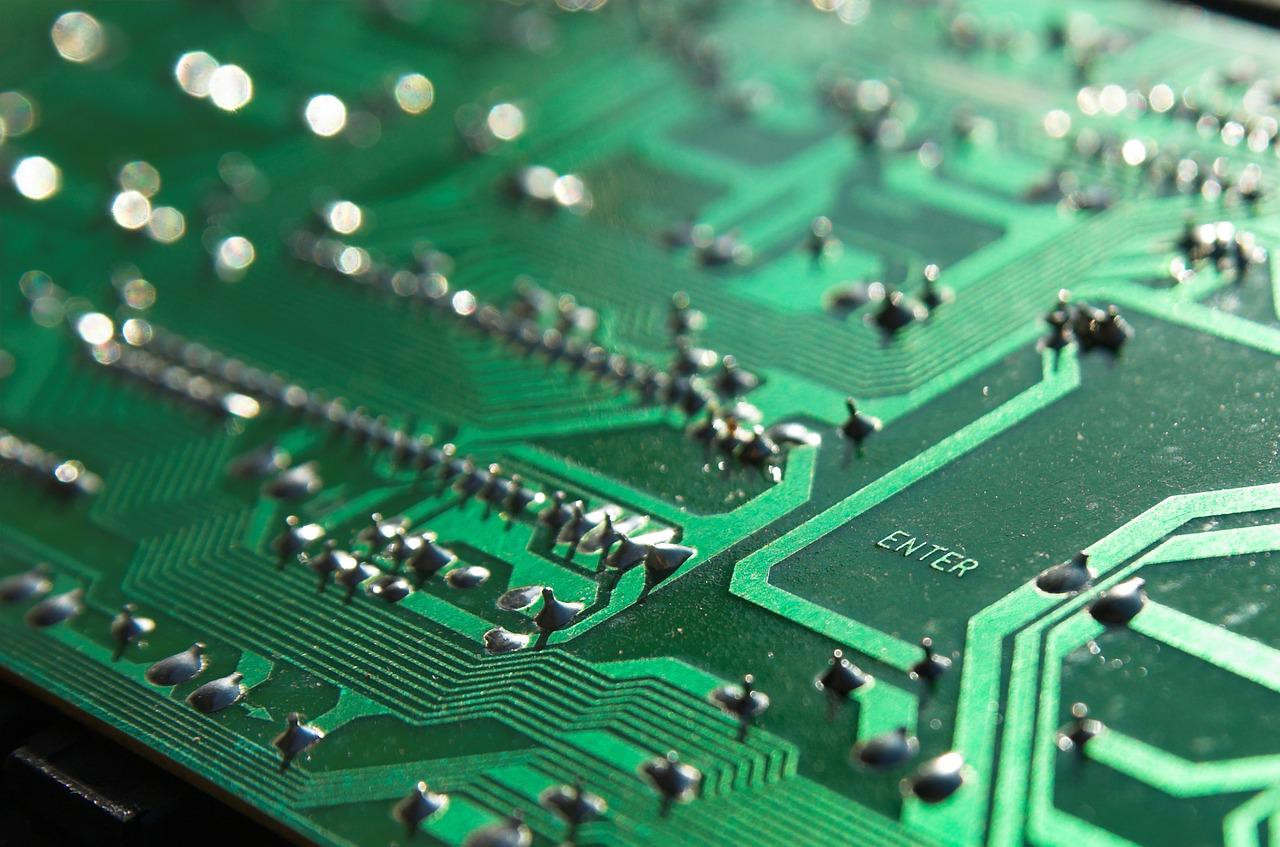
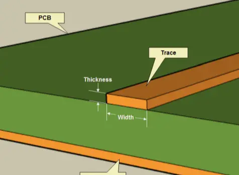
PCBs (Printed Circuit Boards) are the most important part of any electronics product or project or a building block, made of a sandwich of a few different materials, for a basic 2 layer 1.6mm board you would generally have a stack-up of Top Solder Mask, Top Copper Layer, Core (FR-4), Bottom Copper Layer and then Bottom Solder Mask, the number of copper layers will increase proportionally with the number of layers. PCBs have lots of little copper tracks to conduct the power.
They have two complementary functions:
- electrically and mechanically affix them to the PCB which can also aid in thermal conductivity
- providing reliable electrically connections and reliable open circuits along with controlled impedance for high speed traces or RF
Nowadays we have a large choice of PCBs between standard Rigid boards, Advanced Rigid boards, flexible boards, Rigid-flex boards, and Aluminium boards.
PCBs can range from a single layer to 100 layers. Most phones and laptops use upwards of 16 layers to accommodate for lots of signals along with different surface finishes, like ROHS Lead-free, leaded HASL, ENIG Immersion gold or Immersion Silver and even hard gold!
In this tutorial, I’m going to explain what are all the types available from PCBWay for quick manufacture. I’ll also suggest the default PCB manufacturing options in order to have a standard configuration that will fit the common needs of a beginner with a simple board.
PCB Manufacturing Options
Once you have designed your PCB (a tutorial is available from my Getting your First PCB with Raspberry PI and Fritzing article), you will need to decide on a number of options for your board. The main are below explained, using as reference the board example shown in the above mentioned tutorial.
Board Type
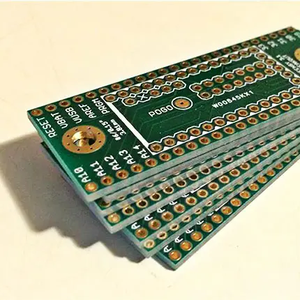
The first of PCB manufacturing options, board type is the different types, for example, single layer board, double layer board, Flex PCB, Rigid-flex. All of these different types have different uses: for example, most PCBs are single, double layer boards which is a non-flex board, the flexible board is like an FFC cable. With a flexible base with traces and components soldered, rigid-flex is a board with parts that are rigid and flexible parts to connect each rigid part.
The default type, for most projects is single or panel, our reference is a single board.
Layers
The number of conductive layers. The layer’s number depends on how complex the PCB design is. If this has connections that are crossing, your design must foresee more layers and the user will provide a design for each layer.
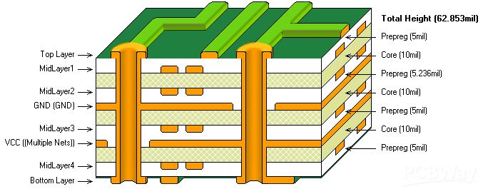
The default value, for projects like our reference above, most designs nowadays are 2 or more layers.
Material
Base material for the PCB. FR-4 is the cheapest material, but it has lower conductivity compared to the others. Aluminium is more expensive than FR-4 but is only mainly used on PCBs requiring large heat capacity, like a torch with lots of hot LEDs. Rogers is very important when you need low electrical signal loss: it can improve impedance control and has better performance when carrying high frequencies. Copper is similar to Aluminium board but has better thermal capacity.
The default material, for most projects, is FR-4, our reference is FR-4.
FR-4 TG: Only applicable to PCBs using FR-4 as base material. FR-4 TG is the glass transition temperature for the core material, PCBWay is offering TG150-160 for free instead of TG130-140. The meaning of TG or glass transition temperature is when the internal fibreglass turns from a solid state to a soft and rubbery state. This is important for any high heat application.
The default TG, for most projects, is TG130-140 but with the free upgrade by PCBWay you can get TG150-160 free of charge.
Thickness
Thickness is how thick your board is. This value doesn’t change when ordering PCBs apart from if you have an edge connector where the pins are on either side where thickness is vital. If you have an edge connector consult the datasheet for information. Layers can affect the thickness: for example, a 100 layer board cannot be 0.8mm
The default thickness, for most projects, is 1.6mm
Min Trace Spacing
This means minimum width between any conductors between two adjacent traces. The smaller the number you go the more expensive it gets.
The default Min Track Spacing, for most projects, is 6/6mil, but for high density boards changes can be made.
Min Hole Size
This means what is the smallest hole size on your PCB for mounting, etc. This excludes vias but includes any other drills.
The default Min Hole Size, for most projects is 0.3mm.
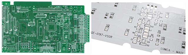
Solder Mask
This is the colour of the mask on the PCB. This is purely cosmetic unless you choose no solder mask that may cause shorting when soldering. There are generally no cost differences for the standard colours like green, red yellow, blue, white and black. There can be a lead time increase for any colour other than green due to the longer drying process.
Moreover, if you want to make your design more special, PCBWay also provides novel solder mask like pink, grey, orange and transparent and so on.
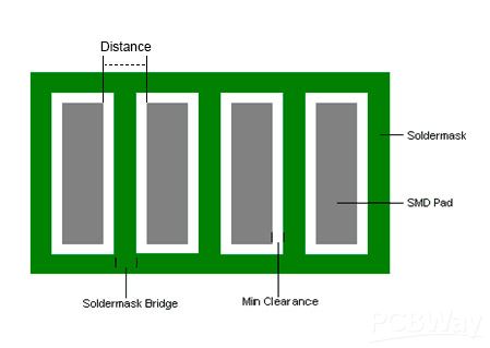
The default Solder Mask colour, is green for most projects but as stated above whichever you wish.
Silkscreen
This is the colour of the ink printed on the PCB to identify components. Similar to a solder mask, this is purely cosmetic, but removing silkscreen entirely can incur adverse effects, eg. Do not know where to place components during placement.
The default Silkscreen colour, is white for most projects but purely cosmetic.
Edge Connector
This enables being able to bevel the edge connector and plate just the connector with a better surface finish like hard gold. If you choose hard gold you are able to choose the thickness of the gold.
The default Edge Connector, isn’t needed for most boards and if you need this you will know exactly what you will need.
Surface Finish
This is what metals will be added to pads to improve solderability. When choosing these options tick the setting that says: Tick means you accept we might change “HASL” to “ENIG” at our discretion without extra charge.
Via Process
This is useless for most boards if you are using Gerbers as, when being manufactured, the Gerbers are more important than these settings. This is a mostly redundant setting so leave it whatever it sets as it will not impact the PCB.
Finished Copper
This is how thick the copper is on the board. Is measured in ounces, so 1oz is 1oz per 1 foot of PCB material.
The default Finished Copper, is 1oz for most projects
Ordering The PCB
In this chapter, we’ll show you how to order your Printed Circuit Board with PCBWay, once you have set the PCB manufacturing options.
At PCBWay it is very easy if you have your Gerbers already in a .zip or .rar file (again, refer to my Fritzing tutorial to see how to export a Gerber file). If your files are in this package, go to https://www.pcbway.com/QuickOrderOnline.aspx and select + Add Gerber File:
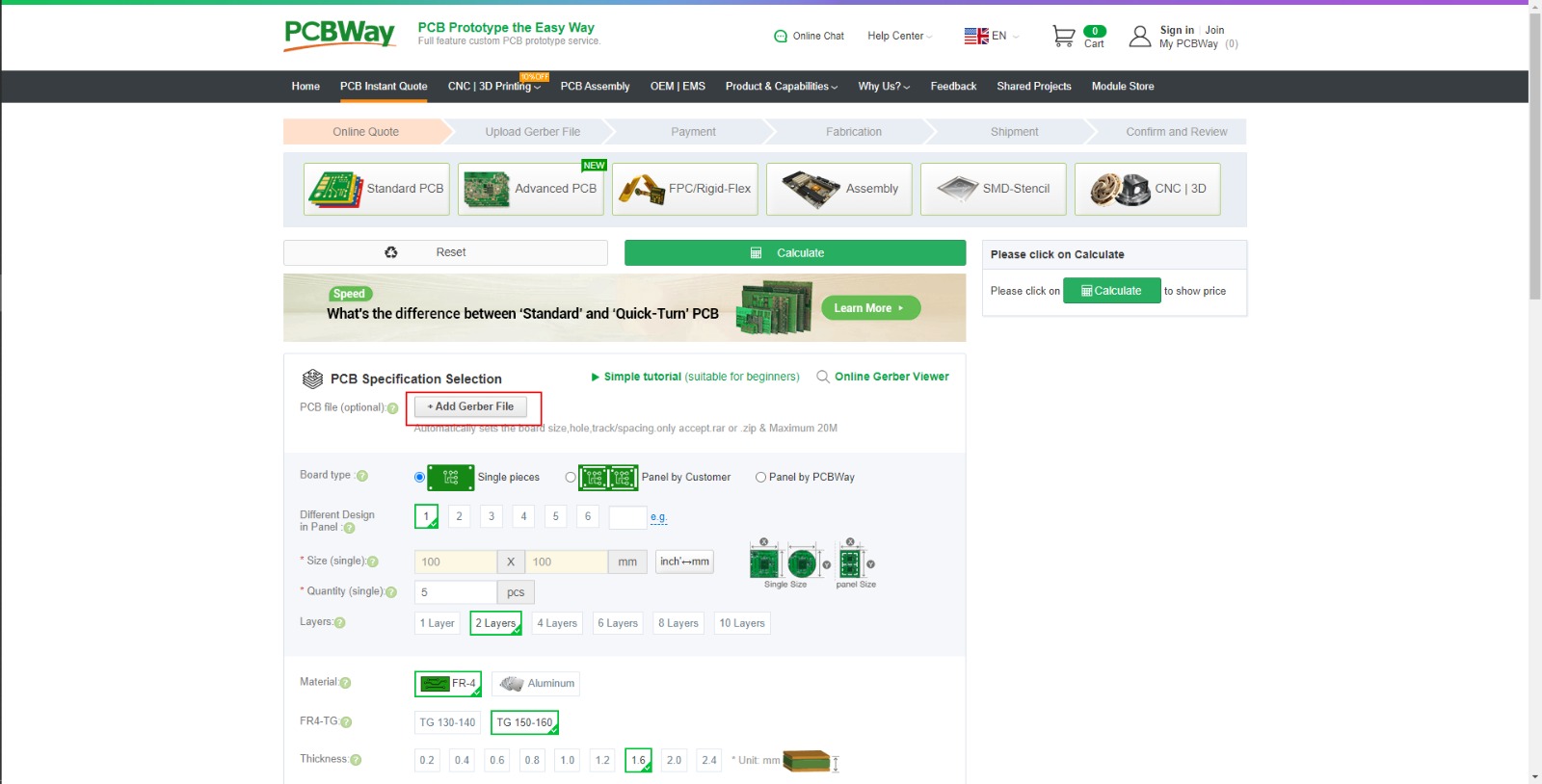
After selecting the .zip or .rar file all the parameters should automatically import. But always check as sometimes these settings can not go into the file. Use the integrated Gerber viewer to make sure they look alright, there can be random discrepancies which you can disregard.
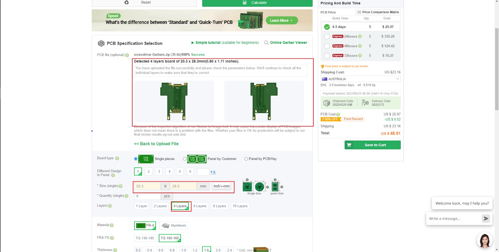
If you are doing a 4 or more layer board it will ask you which files are on each layer. You should be able to find this information in your EDA/design software.
After checking the parameters you can check the estimated shipping cost and then select Save to Cart:
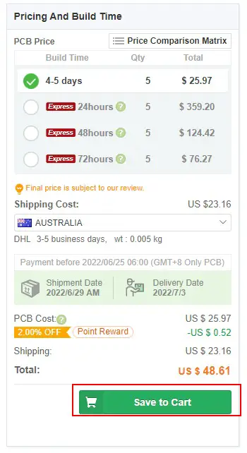
This is where you may have to reupload the .zip/.rar file. You will also find the main PCB manufacturing options summarised:
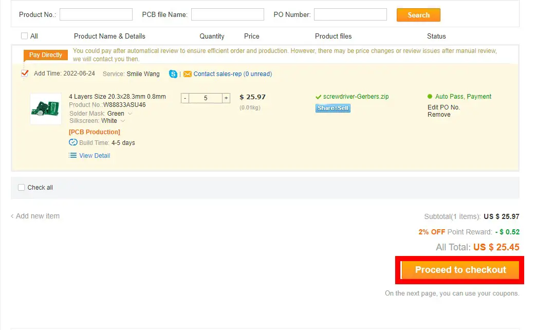
Once doing that you can select Proceed to checkout you should be brought to the screen shown below:
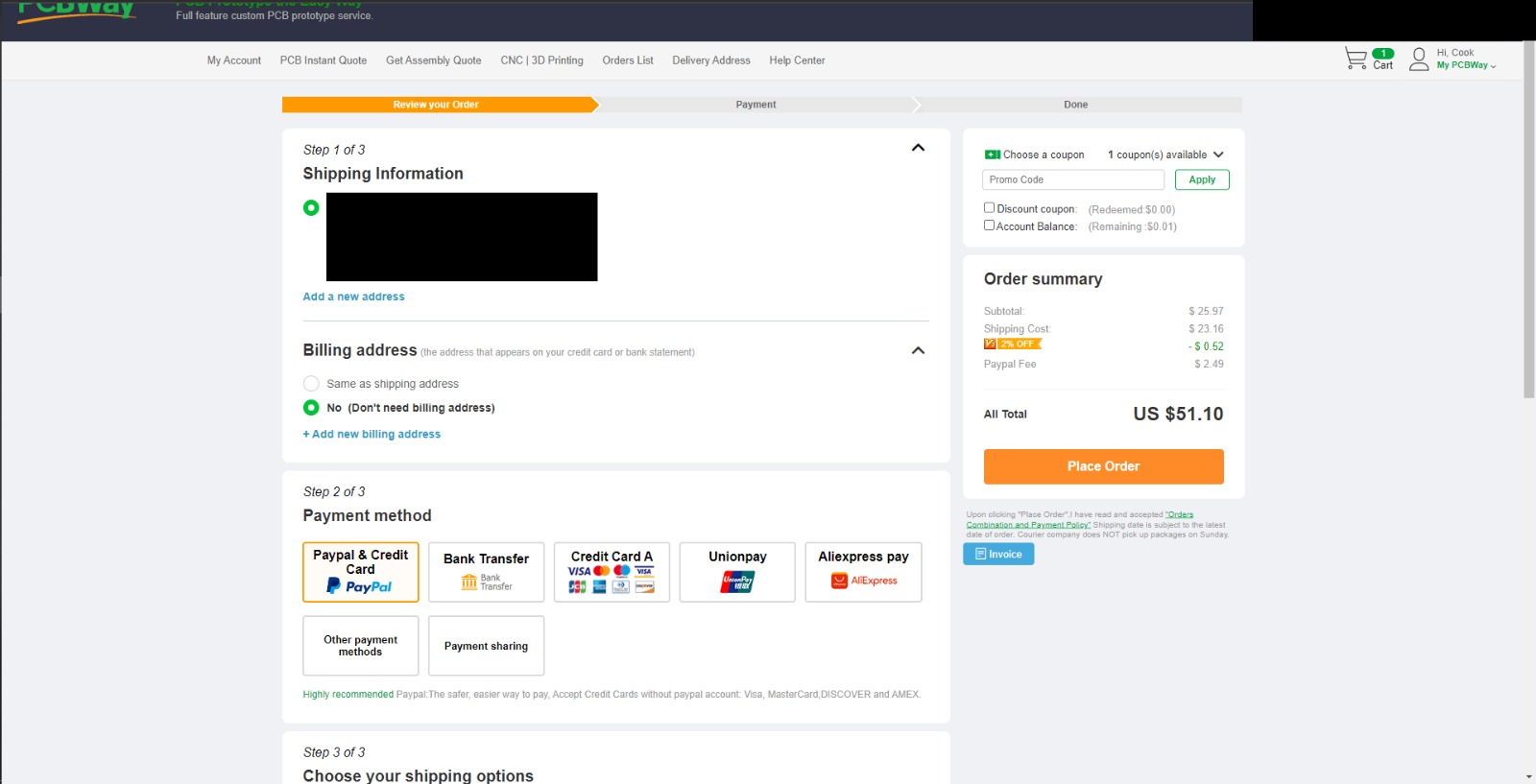
Check your shipping method and if that is set correctly select Place Order. Here you will be brought to the payment screen where you will choose the payment method and then fill out the details. Once you pay for this your order will be placed and manufacturing will start!
You can track the status of manufacturing. 2 layer board should take 24-32 hours, and 4 layers can take 48-72 hours!


The tutorial is more detailed than the official one, and the principle is very good.
Thank you for your feedback, Tony!